
Eighty cores is twice the quantity you possibly can at the moment buy from Intel for as much as $8,099, although it’s solely a 3rd greater than what AMD might promote you for $7,890. However Intel’s flashiest Xeons and AMD’s shiniest Epycs are extra related than you’d think about; they share the identical clock speeds, the identical reminiscence choices, and the identical TDPs. AMD has an higher hand in PCIe connectivity, however Intel’s received higher on-chip connectivity, and so on.
Sapphire Rapids, Intel’s fourth-generation Xeons, share extra rising applied sciences with GPUs than with different CPUs. Nvidia’s five-figure A100, for instance, is the one GPU to supply as much as 80 GB of HBM2e reminiscence. Sapphire Rapids has 64 GB of HBM2e onboard (and eight lanes of DDR5 reminiscence, too). The A100 was the primary GPU to help BF16 computation. Sapphire Rapids will help BF16, too.
Sapphire Rapids additionally has PCIe 5.0, a brand new core structure referred to as Willow Cove, the 10nm Enhanced SuperFin node, and the brand new LGA4677-X socket on its resume.
All that is public info that Intel has divulged, largely deliberately. Intel had begun sampling Sapphire Rapids to companions by the tip of final yr, Intel’s now-former CEO Bob Swan mentioned to buyers in January. A number of sources have mentioned that the pattern fashions had 28 cores enabled.


The story takes a violent flip
On the finish of January, an everyday leaker on the Chinese language website Bilibili gained possession over one of many disseminated samples. He took some pictures, then delidded the processor in probably the most terrible approach doable. Twenty seconds into this clip, he places the processor in an everyday bench vice and simply begins cranking. Earlier than the minute mark, he’s heating it over a gasoline stovetop flame, after which – brace your self – he by chance drops the processor into the flame. (When you’re curious, an oven is often thought of greatest apply, partly to keep away from this subject.)
Afterward, the warmth spreader comes off fairly simply. An post-mortem reveals that the warmth spreader was soldered to the die utilizing indium, like Rocket Lake.
Beneath the warmth spreader was a quad-chiplet formation. It’s theorized, however not with a lot certainty, that Intel is utilizing EMIB (embedded multi-die interconnect bridge) or Foveros to attach the chiplets and the HBM2e reminiscence to achieve an inter-chip bandwidth benefit over AMD’s Infinity Cloth.

Leaker commits an atrocity
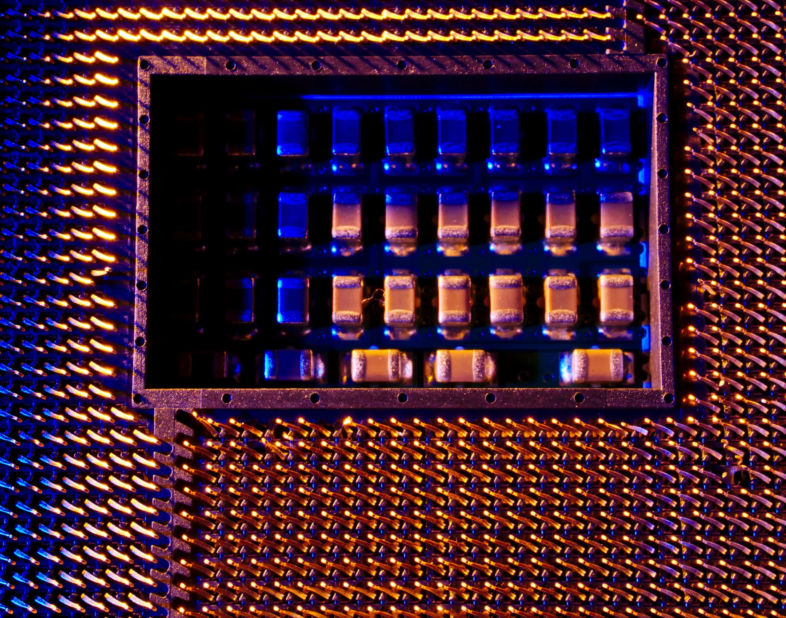
Final week, the leaker pulled all 4 of the chiplets off the substrate, then dissected them. It seems as if he efficiently eliminated the HBM2e chips from three of the chiplets. The fourth… it’s greatest to not look.
Eradicating the HBM2e chips revealed the cores beneath. From the appears to be like of it, every chiplet accommodates twenty cores organized in a 5 by 4 grid. There additionally appear to be a number of controllers and probably interconnect arrays across the perimeter of every chiplet.
The twenty cores took the leaker without warning. It had been leaked, repeatedly, that Sapphire Rapids would prime out at 56 cores. If that had been the case, then Intel can be disabling six of the twenty cores on every chiplet, a proportion unprecedented in a flagship mannequin. It’s doable that the 56-core leaks had been merely fallacious, and it’s additionally doable that not all the preparations that seem like cores are the truth is cores. Essentially the most miserable risk is that Intel’s new node has an absurdly excessive failure charge.


Picture credit score: Michael Dziedzic, Yuuki_AnS
Source link


/dividend_184030710-17e9ceeace14496e9737c65fde0a3701.jpg)
